This has been copied from my old website from circa 2021.
CD32 Motherboard
Information on the CD32 main board
Some information comes from the CD32 service manual..
The system consists of a 4 layer PCB for the main board and 2 additional PCBs, one for the Audio/LEDs and one for the CD-ROM drive.
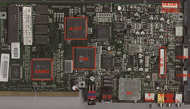
The motherboard for the Amiga CD32 is roughly 6″ by 12″ and is a four layer board. On the main PCB – is a 14MHz 68EC020, the AA chipset, an ASIC called Akiko, a DAC for playing standard CD audio, and a small amount of EEPROM.
Akiko is a 160-pin PQFP surface-mounted device containing most of the remainder of the logic necessary m the Amiga CD32. It includes the CD-ROM control logic and the system timers. The EEPROM is 8K bits, and designed for storing Settings, high scores, bookmarks, etc., on the Amiga CD32.
In addition to the AA chips, Akiko, the CPU and the EEPROM/ the main board contains 2MB of DRAM as Chip RAM. A PAL or NTSC modulator is also included on the main board.
The Compact Disc DAC is a standard 18-bit, 8x oversampling DAC. Along with the superb audio quality of the DAC, the Amiga CD32 expansion connector has digital audio input capability in order to mix an external source such as MPEG audio with the CD audio and Amiga audio.
There were two released version of the PCB, version 3 was the standard PCB for PAL/NTSC machines. A special version 4 PCB was made for the French market (they use a SECAM TV system) The only difference between the two types is the video encoder.
It is reported that the On/Off switch is from the old C64 production line and is liable to cause problems, see the CD32 PSU Information page for more information.
CD32 Memory Map
This information comes from the CD32 service manual.
CD32 CDROM drive information
CD32 CD-ROM Subsystem
Here is some information on the internal drive of the CD32.
This information comes from the CD32 service manual.
A separate PCB (2 layer) contains the CD electronics. This board contains the RF amp and servo chip, the audio DSP chip, and a small microcontroller for controlling the servo, focus, and communicating with the main CPU. The main CPU and RAM perform any prefetching/ buffering and ECC as necessary.
The mechanism for the Amiga CD32 is a Sony KSM-2101BAM. The KSM-2101BAM has no drawer, or drawer motor. It is simply a spindle motor, traverse motor, and optical pickup. Chinon will provide the drive PCB. The electronics are based on the Sony CD chipset, which support double-speed operation. The microcontroller firmware has changed slightly in this version of the drive to (1) remove the firmware to control the drawer, and (2) revise the communications protocol to use a new 3-wire channel instead of the older 6-wire channel (to save pins on the ASIC) and (3) support multi-session discs (which is useful for PhotoCD support).
The software driver for the CD subsystem has been converted to run entirely on the 68EC020. The software also supports Akiko and its new DMA. This driver incorporates all the prefetching tricks and double-speed support completely from the 68EC020. It also supports both Mode 1 and Mode 2 (Form 1 and 2) discs. This is required to read all types of CD media called out in the Philips Yellow Book. This includes CD-I discs, PhotoCD® discs, and MPEG discs.
CD32 PSU replacement
This is left here for reference, it was written before I’d designed the ATX PSU adaptors I sold until 2023.
PC Power Supplies as replacements/upgrades
It is quite common now to replace the under rated original Amiga PSU with a PC one, asPC PSUs start at 135W and go to over 500W it is easy to see why.
There are minor differences in using an AT or ATX PSU to power an Amiga and leter on I will explain the witing.
AT PSU
Not really used in PCs since 1998/99 due to the PC requirement that software can switch
the PC off (or a Microsoft plan to stop their software crashing).
Normally found in old/dead PCs (they have some uses). To hook it upto your Amiga you will need to note wiring of the square DIN plug (check the underside of the PSU) and then cut it off.
Commodore never seemed to use the same colour code in all Amiga models so you will need to check your wiring with a multimeter. See the power connector section for more details.
Once you have wired up the Amiga cable, connect a 21W car bulb across the +5V (RED) and 0V (BLACK) wires. This will provide a suitable load to turn on the PSU and you can then ensure you have the right voltages going to the right pins before pluging into your Amiga.
If all seems well, connect to your Amiga and switch on!
Important note. Modern PSUs have what is called crow bar protection, if you short it out or wire up backward, to cause a large power surge, it will switch off. Don’t count on this, double check your wiring!
Some AT PSUs had the mains switch inside the PSU housing, that is fine. Some had a mains lead that went to the power switch on the front of the PC case. If possible avoid this type unless your Amiga case has a suitable power switch.
Final note, do not open a PSU case. Due to their operation, a typical computer power supply can have upto 400V DC stored within for a considerable time after power off. If you inadvertantly touched the wrong part you could be killed!
ATX PSU
This is the type of PSU found on all modern PCs and within cases. There are 2 important differences to the AT PSU. The following conditions must be met.
1) You need to have about a 1.0 Amp load on the 5V supply for it to work.
2) You need to connect the PS-ON line to ground for the PSU to switch on.
Condition 1 is easily satisfied, an Amiga uses enough current on the 5V supply.
Condition 2 is a bit trickier.
It is possible to create a simple circuit to use the push to make power button of
an ATX case. A simpler solution is to bare back the insulation of the PS-ON wire
(normally green) and of a ground wire (black). Then either twist them together or
add a link wire, solder it an insulate it. Now when you use the mains switch on
the back of the ATX PSU, it will switch on the PSU.
the circuit to utilise the PC front panel switch is available here
CD32 Expansion port
Update & Notes
The original notes on the CD32 expansion port were released in 1995, they left out a few pins, which I have added to the list below. there is built in support (I think) for a 68030 processor on this expansion connector, previously these signals were marked as no connect (n/c).
The mating connector is a 182 way MCA connector which is possible to obtain.
#####################################################################
##
CD32 Expansion port info. 1994-07-05 by Anders Stenkvist                    ##
##      Updated 19th April 2002 by Ian
Stedman
##

#####################################################################

 2                         84___86                        182
 |--- TOP
 ////////////////////////////   ////////////////////////////
v
/==========================/   /==========================/
^                          ^   ^                          ^
^
1                         83   85                        181    |___ BOT

Note DGND = digital GND
     VCC  = +5V
     A * after a signal denotes active low.

Pin
#   Name           Comment
===========================================================================
Pin  1   A31            Probably not connected since 68EC020
 |       |              |
Pin  8   A24  Probably not connected since
68EC020
Pin  9   DGND
Pin 10   VCC
Pin 11   A23            Address bus
 |       |              |
Pin 18   A16            |
Pin 19   DGND
Pin 20   VCC
Pin 21
A15            |
 |       |              |
Pin 28   A8             |
Pin 29   DGND
Pin 30   VCC
Pin 31   A7
|
 |       |              |
Pin 38   A0             Address bus
Pin 39   DGND
Pin 40   VCC
Pin 41   D31            Data bus
 |
|              |
Pin 48   D24            |
Pin 49   DGND
Pin 50   VCC
Pin 51   D23            |
 |       |              |
Pin 58
D16            |
Pin 59   DGND
Pin 60   VCC
Pin 61   D15            |
 |       |              |
Pin 68   D8             |
Pin 69   DGND
Pin 70
VCC
Pin 71   D7             |
 |       |              |
Pin 78   D0             Data bus
Pin 79   DGND

Pin 80   VCC
Pin 81   IPL2*          Interrupt Priority
Level 2 (68020 signal)
Pin 82   IPL1*          |
Pin 83   IPL0*          Interrupt Priority Level 0
Pin 84   IPEND  Interrupt pending
Pin 85   RST            Request to send (RS232 port)
Pin 86   HALT*          Processor Halt
Pin
87   ECS*           Not implemented on 68EC020 (68030 signal)
Pin 88   OCS*           Not implemented on 68EC020 (68030 signal)
Pin 89   SIZE1          Indicates number of bytes remaining to transfer
Pin 90   SIZE0          Indicates number of bytes
remaining to transfer
Pin 91   AS*            Adress strobe
Pin 92   DS*            Data strobe
Pin 93   R/W*           Read/Write
Pin 94   BERR*          Bus Error
Pin 95   STERM*  68030 STERM (reserved)
Pin
96   AVEC*          Autovector request during interrupt acknowledge
Pin 97   DSACK1*        Data transfer and size acknowledge
Pin 98   DSACK0*        Data transfer and size acknowledge
Pin 99   CPUCLK_A CPU Clock 14 MHz
Pin100   E              Peripheral
Enable Clock
Pin101   DGND
Pin102   VCC
Pin103   FC2            Function codes
Pin104   FC1            Function codes
Pin105   FC0            Function codes
Pin106   RMC*  Read Modify cycle
Pin107   CIIN*  68030 CIIN
(Reserved)
Pin108   CIOUT*  68030 CIOUT (Reserved)
Pin109   CBREQ*  68030 CBREQ (reserved)
Pin110   CBACK*  68030 CBACK (Reserved)
Pin111   CPU_BR*        CPU bus request
Pin112   EXP_BG*        Expansion bus grant
Pin113   CPU_BG*        CPU bus grant
Pin114
EXP_BR*        Expansion bus request
Pin115   CPU_BGACK* CPU bus grant Acknowledge
Pin116  EXP_BGACK* Expansion bus acknowledge
Pin117   PUNT*  Back off signal to console
Pin118   RESET*         General  RESET
Pin119   INT2*          Generate a level 2 interrupt
Pin120
INT6*          Generate a level 6 interrupt
Pin121   KB_CLOCK*      Keybord clock
Pin122   KB_DATA*       Keybord data
Pin123   FIRE0*         Fire buttons
Pin124   FIRE1*         |
Pin125
LED*           Power On Led
Pin126   ACTIVE*        CD Drive active led
Pin127   RXD*           Serial data in
Pin128   TXD*           Serial data out
Pin129   DKRD*          Disk Read Data
Pin130
DKWD*          Disk Write Data
Pin131   SYSTEM         (Reserved)
Pin132   DKWE*          Disk Write Enable
Pin133   CONFIG_OUT*    Zorro config signal
Pin134   CONFIG_IN* Zorro config signal
Pin135   DGND
Pin136   +12V
Pin137
DGND
Pin138   +12
Pin139   17MHZ         CD-Drive/CD-DAC clock
Pin140   EXT_AUDIO*    External audio enable
Pin141   DA_DATA       CD-Data
Pin142   MUTE*         Audio mute signal
Pin143   DA_LRCLK      CD-Data Left Right clock
Pin144
DA_BCLK       CD-Data bit clock
Pin145   DGND
Pin146   VCC
Pin147   DR            Digital Red
Pin148   DG            Digital Green
Pin149   DB            Digital Blue
Pin150
DI            Digital Intensity
Pin151   PIXELSW_EXT*  External genlock pixel switch (Video)
Pin152   PIXELSW*      Genlock Pixel Switch (Video)
Pin153   BLANK*        Video blanking signal
Pin154   PIXELCLK      Pixelclock for manipulating RBG data
Pin155   DGND
Pin156
VCC
Pin157   CSYNC*        Composite sync
Pin158   CCK_B         Color clock ?????
Pin159   HSYNC*        Horizontal sync
Pin160   VSYNC*        Vertical sync
Pin161   VGND          Video ground
Pin162
VGND          Video ground
Pin163   AR_EXT        External Analog Red
Pin164   AR            Analog Red
Pin165   AG_EXT        External Analog Green
Pin166   AG            Analog Green

Pin167   AB_EXT        External Analog Blue
Pin168   AB            Analog Blue
Pin169   VGND          Video ground
Pin170   VGND          Video ground
Pin171   NTSC*        NTSC
Pin172
XCLKEN*       Enable External video clock (Genlock)
Pin173   XCLK          External video clock (Genlock)
Pin174   EXT_VIDEO*    Disable internal video interfaces
Pin175   DGND
Pin176   VCC
Pin177   AGND
Pin178   +12
Pin179   LEFT_EXT      External Left sound
Pin180
LEFT          Left sound
Pin181   RIGHT_EXT     External Right sound
Pin182   RIGHT         Right sound


NOTE: Signals with a _EXT suffix are intended for the CD32 FMV module.